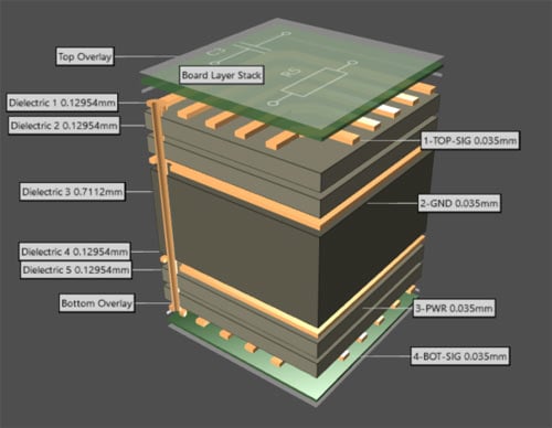
Balancing layers in your PCB layout stack-up, which both layer surfaces and cross-sectional structure of the circuit board are reasonably symmetrical.
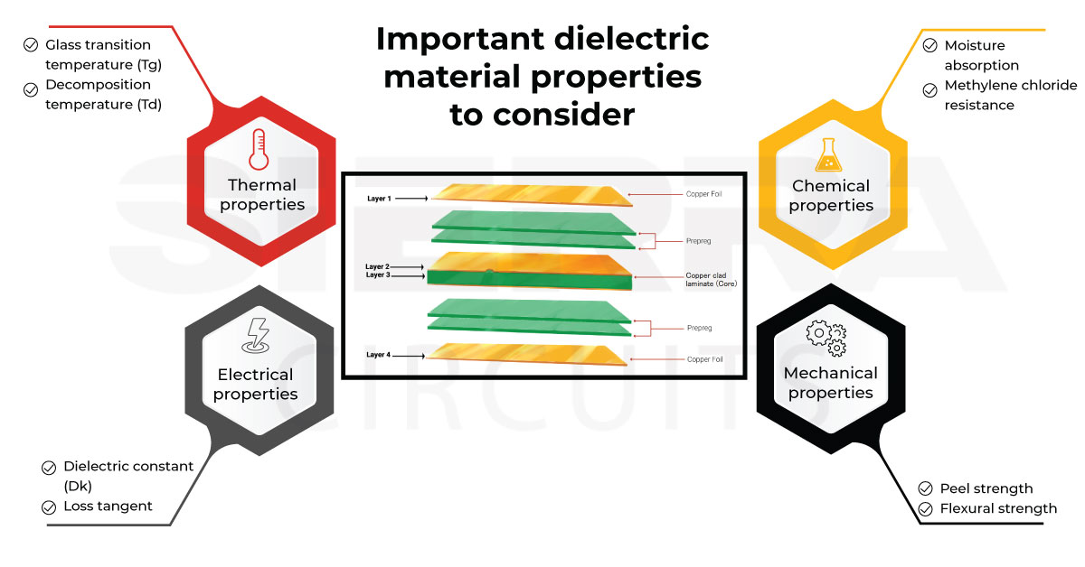
PCB Substrates: Knowing PCB Dielectric Materials

The Most Common 2-Layer PCB Design Mistakes and How To Avoid Them
Methods for Balanced PCB Stackup Design – PCB HERO
PCB Layers Explained: Everything You Need to Know

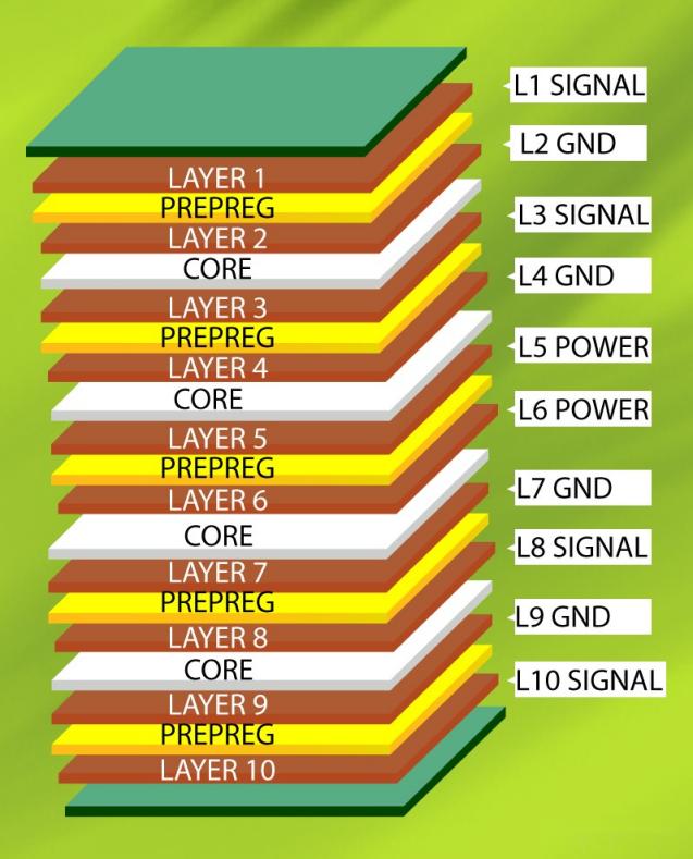
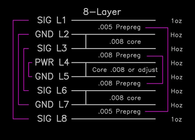
How to Plan Multilayer PCB Stackup - RAYPCB

EasyEDA Std Tutorial
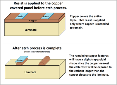
PCB Copper Thickness: General Guidelines and Tips

Balanced and unbalanced PCB layer stack-up for controlling radiated emissions
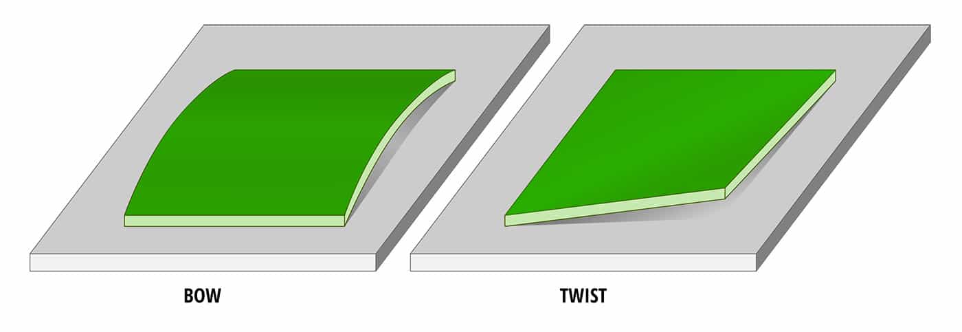
Understanding Bow and Twist on a PCB - Eurocircuits
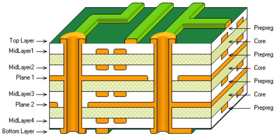
An Overview of Layer Stack Management in PCB Design

Gigabit Ethernet 101: Basics to Implementation, Blogs

Design Guidelines for Error Free IPC Class 3 PCBs
Epec's Blog

EasyEDA Std Tutorial

PCB Trace and Pad Clearance: Low vs. High Voltage, PCB Design Blog


)