The complete guide to PCB pad :types, size, spacing, repair and comparison - IBE Electronics
$ 10.99
4.5(749)In stock
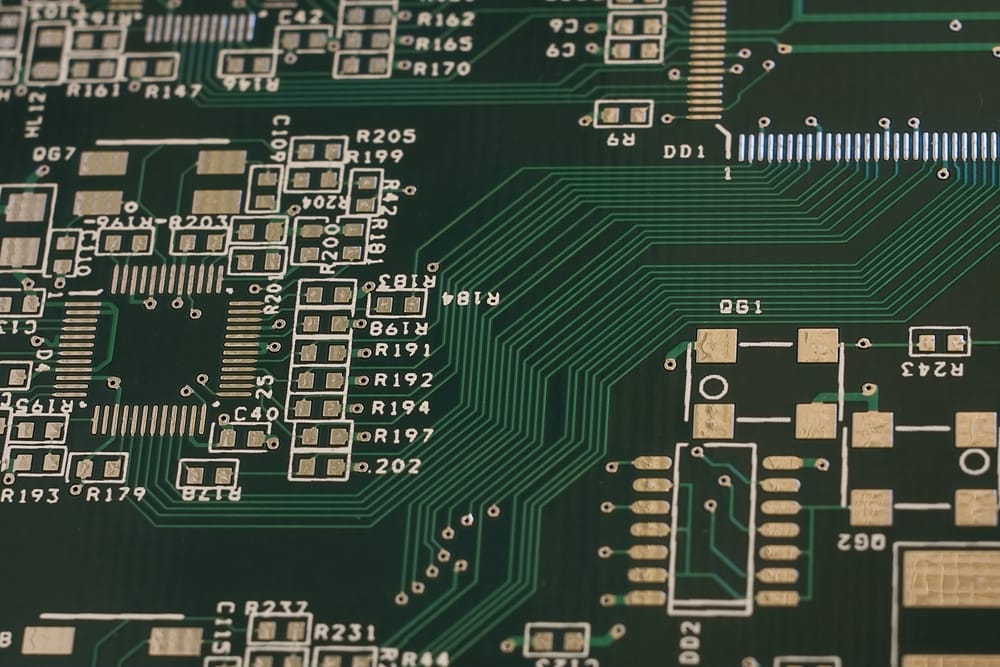
Soldering is one of the most important processes in PCBA processing. On printed circuit boards, electrical connections to all components are made via PCB pads. The PCB pads are a very critical part of the PCB that determines where components are soldered on the PCB.The size, shape, and position of pads in a PCB directly depend on the manufacturing quality of the board. Today we will take a look at the PCB pad in SMT soldering. Soldering is one of the most important processes in PCBA processing. On printed circuit boards, electrical connections to all components are made via PCB pad.
PCB Layers: Everything You Need to Know
Your Guide to Flexible PCB Design & Layout
The complete guide to PCB pad :types, size, spacing, repair and comparison - IBE Electronics
PCB design - your 10-minute guide to create your PCB - IBE Electronics
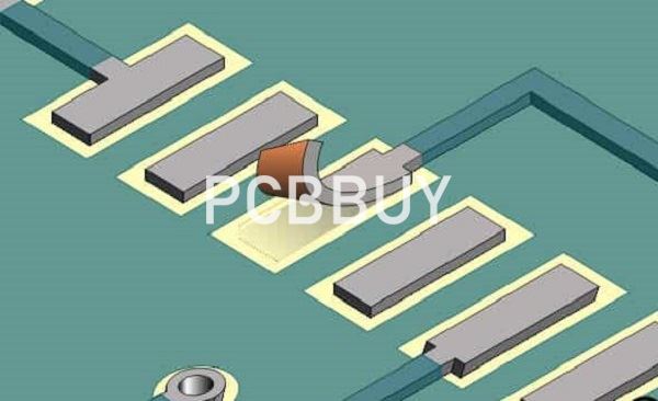
Identifying and Processing Via-In-Pad in PCB Design - JHYPCB
What is Pad to Pad (PP) ?
PCB Pad Size Guidelines with 5 Basic PCB Layout Tips
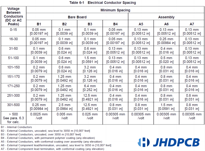
Trace Spacing: A Guide For PCB Design - Jhdpcb
Xiaomi Packs 48-megapixel Camera Into Budget Redmi Note, 55% OFF
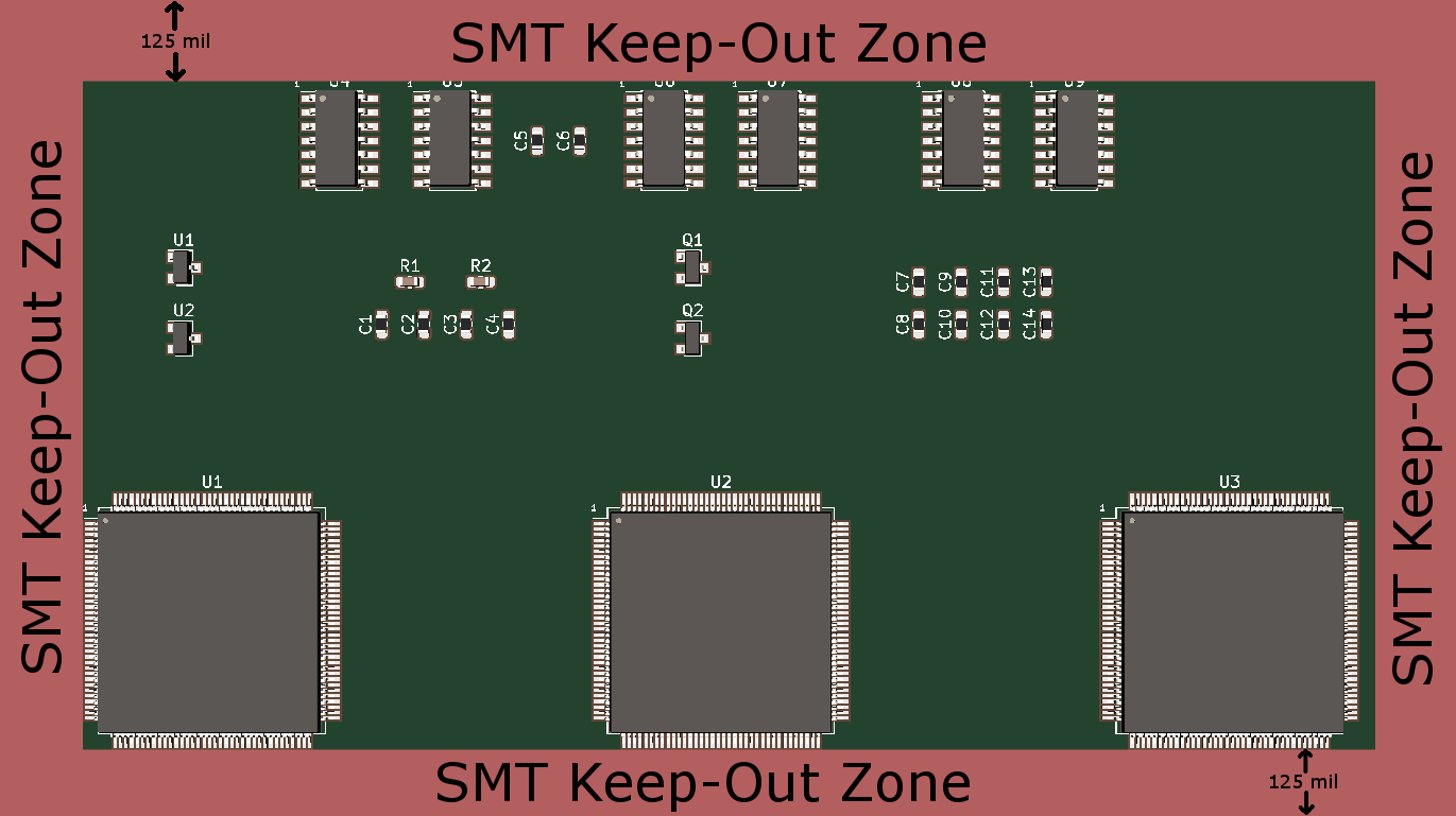
Part-to-Part, Part-to-Hole, and Part-to-Board Edge Spacing
What is the Production Hole Diameter In PCB?
Xiaomi Packs 48-megapixel Camera Into Budget Redmi Note, 55% OFF
What is a PCB pad - different types and design guidelines - PCBA Manufacturers
PCB Pad Size Guidelines: Finding the Proper Pad Sizes for Your Circuit Design