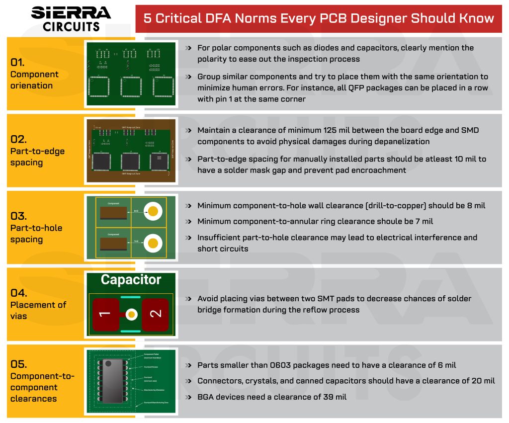
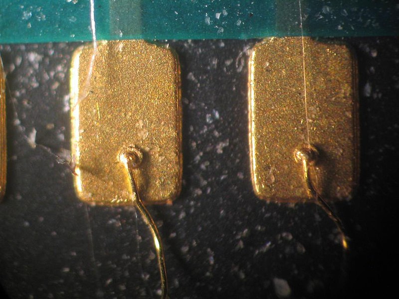
A pad is critical to PCB design as it serves as the designated surface area for electrical contact between the component and the board.
14 Tips For PCB Design For Assembly
Component Placement in PCB Design & Assembly
PCB Basic Knowledge_84
PCB Basic Knowledge_100

How To Repair Damaged /Missing PCB Pads INVISIBLE Fix, 45% OFF
接触焊点- 维基百科,自由的百科全书

What is a Pad in PCB Design and Development? - Absolute

PCB Fab Express on LinkedIn: RAPID PROTOTYPE SERVICE

14 Tips For PCB Design For Assembly

What is a Pad in PCB Design and Development

PCB Basic Knowledge_84
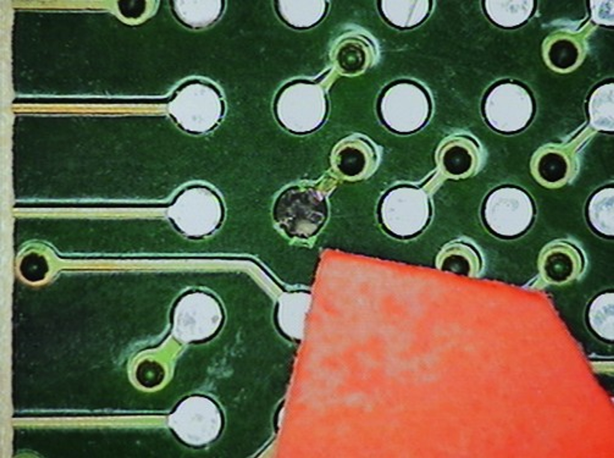
How To Repair Damaged /Missing PCB Pads INVISIBLE Fix, 45% OFF
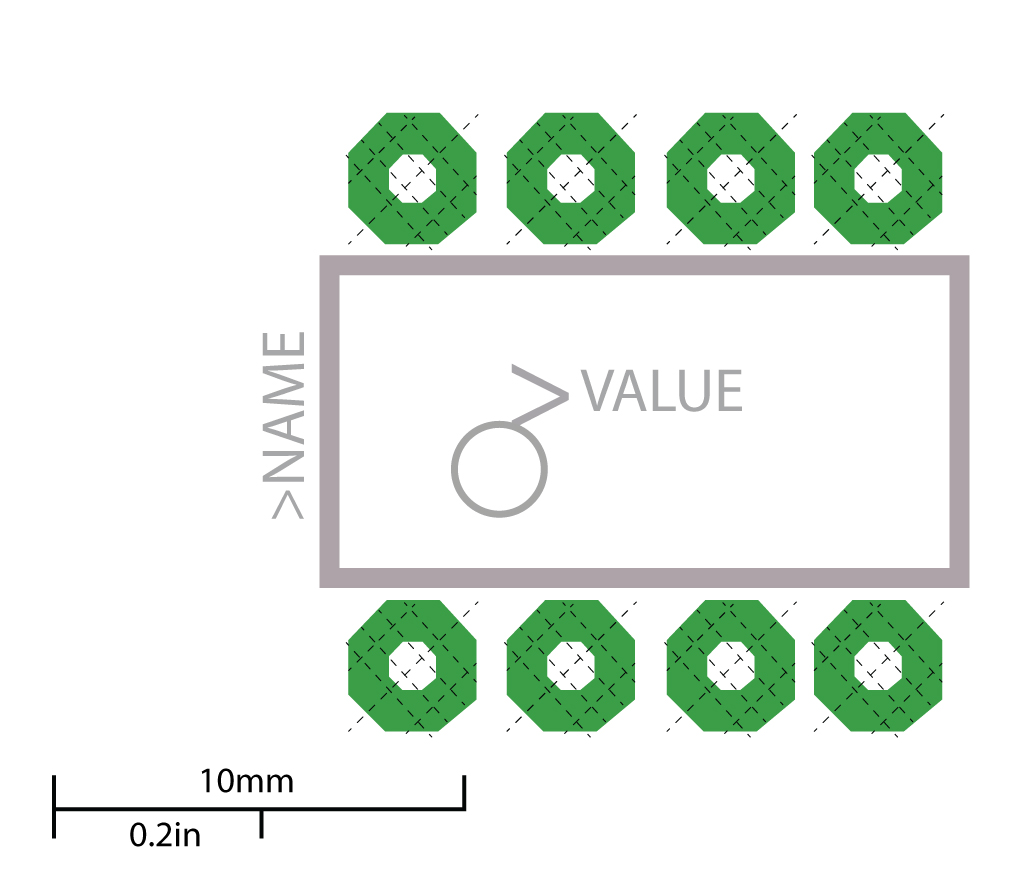
What is a Pad in PCB Design and Development
What is DRC in PCB?