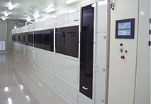
Introduction to application examples, advantages, and standard specifications of electroless UBM formation service
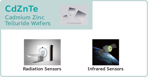
Compound Semiconductor Wafers - InP, CdZnTe -|Special Site of JX Metals

Effect of electric current stressing on mechanical performance of solders and solder joints: A review
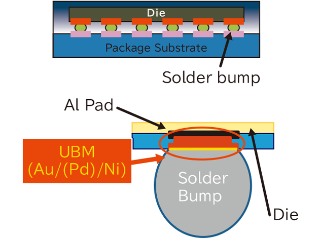
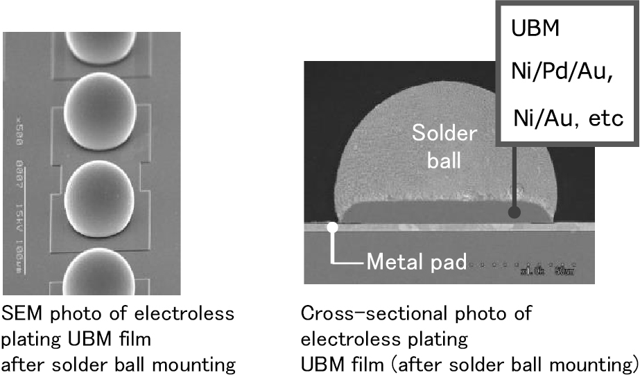
UBM (OPM: Over Pad Metal, FSM: Front Side Metal and Electroless plating) Service - JX Metals
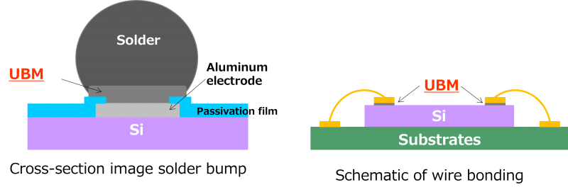
UBM (Under Bump Metallization)

PDF) Proceedings of 4th International Conference in Advanced Manufacturing for Multifunctional Miniaturised Devices (ICAM3D)
総合めっき薬品会社|メルテックス株式会社

ISES USA 2023 - Sponsor Profiles
Our Core Technologies Contributing to Societal Growth and Innovation|JX Metals Corporation
Compound Semiconductor Wafers - InP, CdZnTe -|Special Site of JX Metals
Metal Powders for Additive Manufacturing (3D Printer) - JX Metals

Simulation of current distribution in the solder bump: ͑ a ͒ Solder

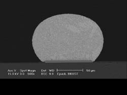
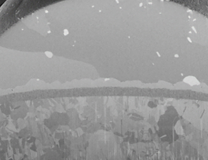
Electroless UBM and solder bump [12, 17]